
Anonymized PCB Layout
Released layout drawing
Anonymized layout with central BGA escape and dense SMD, released with fabrication outputs.
Hardware & PCB
Processing boards with several BGA devices and dense SMD.
Anonymized PCB Layout
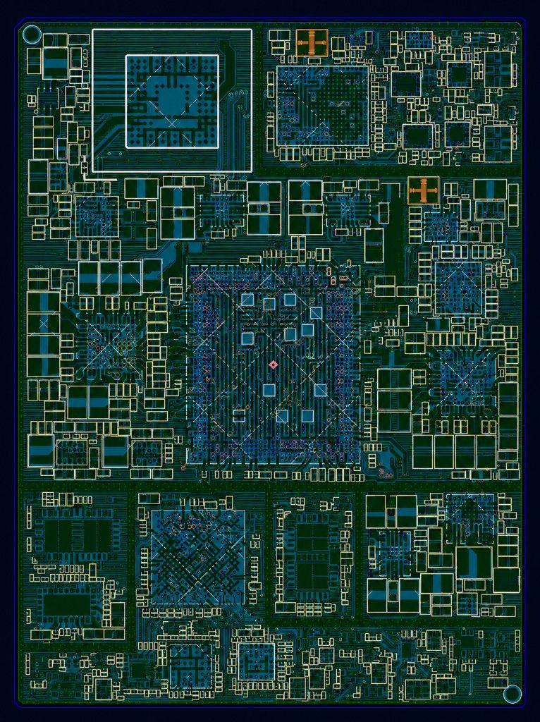
A processing board with several BGA devices and dense SMD. Adjacent escapes share a limited set of routing channels.
Coordinate multiple BGA escape regions without losing reviewable layer transitions.
Yunxin planned the escape regions so they do not take the same channels, then reviewed vias and the manufacturing release.
Anonymized PCB Layout
Anonymized layout with central BGA escape and dense SMD, released with fabrication outputs.