Engineering Capabilities
System architecture, power electronics, FPGA processing, display integration and hardware validation for the same class of programs.
01
System Architecture & Component Selection
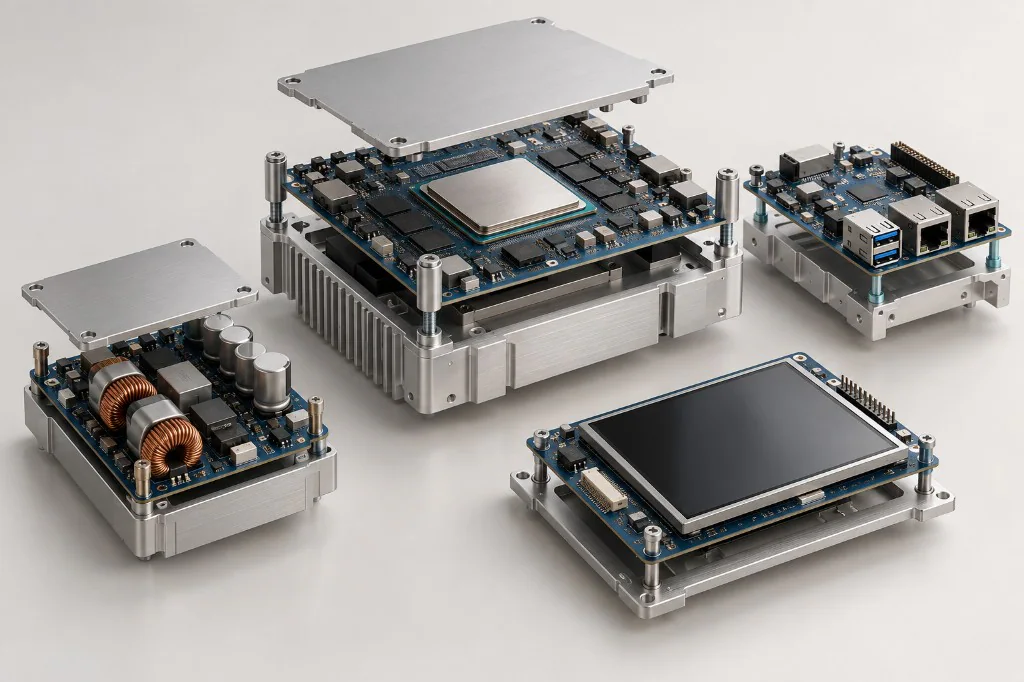
Yunxin turns an application into a workable electronics architecture before detailed design. The work partitions processing, interfaces, power and mechanical limits, then selects devices against bandwidth, package, supply and product life. Interface definitions and the power tree are set with those partitions, so later schematic work starts from one system plan.
-
Requirements & Interface Definition
Break operating conditions into blocks, interfaces and the constraints between them.
-
Architecture & Device Evaluation
Compare devices for bandwidth, power, package and supply, then set the power tree.
-
Risk Assessment & Development Planning
Record interface and power dependencies before schematic and layout work begins.
02
Power Electronics
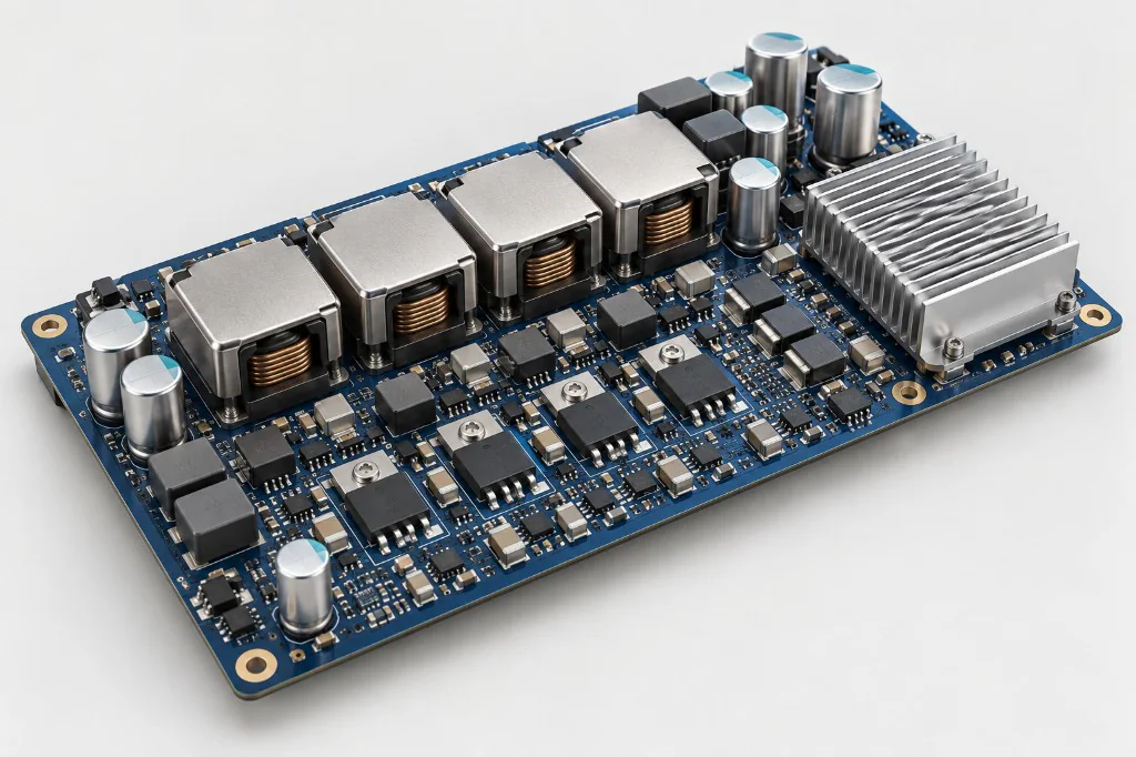
Board-level power work covers conversion, rail definition, control, protection, monitoring and thermal design for compute, display and industrial equipment. Topology and devices follow the load profile and the operating environment, from the first schematic through layout and board evaluation. Startup, transients and fault behavior stay in that plan.
-
Power Architecture & Conversion
Set rails and conversion stages against load current, input range and thermal limits.
-
Sequencing, Protection & Monitoring
Add sequencing, protection and voltage, current and temperature monitoring for the loads.
-
Layout, Thermal Design & Evaluation
Place current paths, switching loops and heatsinking in the PCB, then check regulation on the prototype.
03
FPGA & High-Speed Interfaces
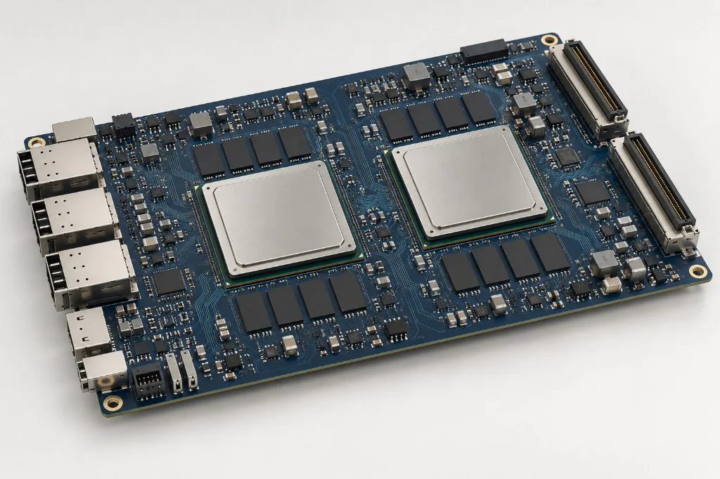
FPGA development covers video input and output, real-time processing, clock domains, memory and synchronized display timing. The pipeline is sized for pixel throughput, latency and the resources of the chosen device. Receive and transmit paths stay on one timing plan, and link behavior is closed during hardware bring-up.
-
Video Interfaces & Link Integration
Integrate video receivers and transmitters with application logic and link timing.
-
Streaming Processing & Memory Architecture
Build streaming pipelines and buffers around throughput, latency and memory bandwidth.
-
Clocking, Synchronization & Debug
Close clock-domain crossings and frame alignment during hardware bring-up.
04
Display & Backlight
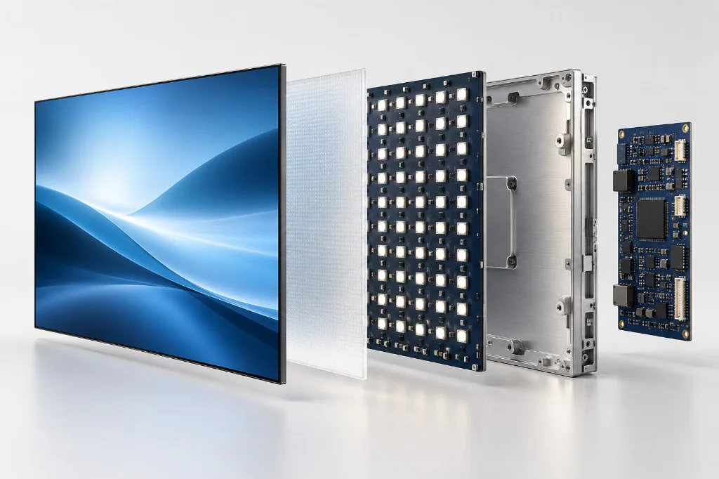
Display work joins panel interfaces, timing, panel power, LED drive and dimming. Video timing and backlight behavior are planned as one system, including local dimming where the panel uses zones. Electrical limits, optical response and heat are considered with the chosen module. The two paths share startup order and brightness control.
-
Panel Interfaces & Display Control
Match video interfaces, TCON signals and panel power sequencing to the module.
-
Backlight Drive & Local Dimming
Drive LED strings or zones and map brightness to the display timing.
-
System Timing & Display Evaluation
Check flicker, brightness steps and startup order on the assembled display.
05
Hardware, PCB & Validation
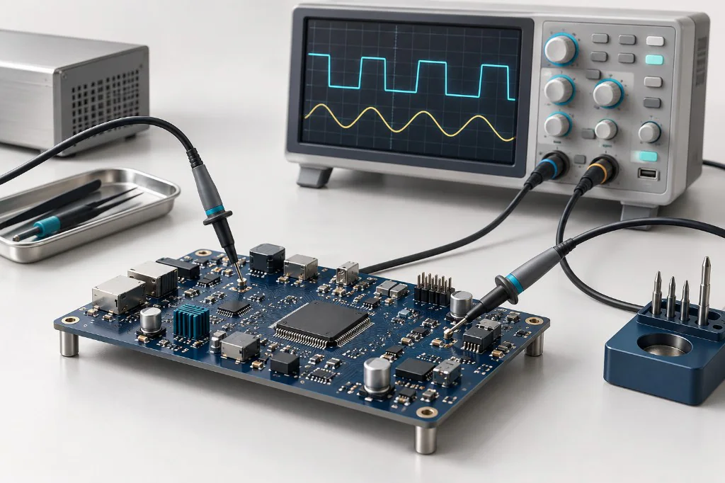
Hardware work carries the architecture into schematics, PCB layout, prototype debug and the files needed for later builds. Layout covers power distribution, high-speed routing, thermal paths and mechanical fit. Fabrication and SMT are coordinated with manufacturing partners in Shenzhen. Bring-up checks rails, clocks and interfaces before the next revision.
-
Schematic & PCB Implementation
Draw schematics and multilayer layouts with stack-up, return paths and test access.
-
Bring-Up & Engineering Verification
Bring up rails, clocks and interfaces, then debug the board under its operating conditions.
-
Prototype Coordination & Design Handover
Prepare fabrication files, the BOM and assembly notes for the agreed build.
Discuss Your Engineering Requirements
Share your application, key specifications and development stage. We can help define the architecture, engineering scope and next steps.