Anonymized PCB Layout
Released layout drawing
Anonymized layout showing perimeter routing channels and large BGA fan-out. Deliverables were defined according to the agreed layout and manufacturing-output scope.
Case Study
Hardware & PCB
Dense digital processing boards with multiple high-pin-count devices.
Anonymized PCB Layout
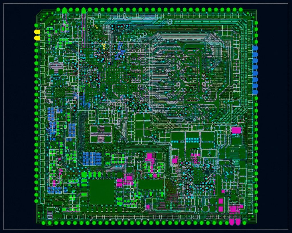
The engineering scope covered constraint definition, BGA fan-out, multilayer channel organization and a DFM-ready release package from a customer-provided schematic.
Organize dense digital routing in a constrained outline while keeping escape paths and return continuity workable.
Allegro constraints were set before dense routing. Fan-out, channel organization and return-path reviews were completed before release.
Anonymized PCB Layout
Anonymized layout showing perimeter routing channels and large BGA fan-out. Deliverables were defined according to the agreed layout and manufacturing-output scope.
Share your schematic, mechanical constraints, interface requirements and expected deliverables.